DESCRIPTION. These products are miniaturized IR receiver modules for infrared remote control systems. A PIN diode and a preamplifier are assembled on a
8 pages
Missing: ricevitore | Must include: ricevitore
131 KB – 8 Pages
PAGE – 1 ============
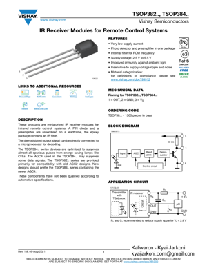
TSOP382.., TSOP384..www.vishay.com Vishay Semiconductors Rev. 1.8, 09-Aug-2021 1Document Number: 82491 THIS DOCUMENT IS SUBJECT TO CHANGE WITHOUT NOTICE. THE PRODUCTS DESCRIBED HEREIN AND THIS DOCUMENT ARE SUBJECT TO SPECIFIC DISCLAIMERS, SET FORTH AT www.vishay.com/doc?91000 IR Receiver Modules for Remote Control SystemsLINKS TO ADDITIONAL RESOURCES DESCRIPTION These products are miniaturized IR receiver modules for infrared remote control systems. A PIN diode and a preamplifier are assembled on a leadframe, the epoxy package contains an IR filter. The demodulated output signal can be directly connected to a microprocessor for decoding. The TSOP384.. series devices are optimized to suppress almost all spurious pulses from energy saving lamps like CFLs. The AGC4 used in the TSOP384.. may suppress some data signals. The TS OP382.. series are provided primarily for compatibility with old AGC2 designs. New designs should prefer the TSOP 384.. series containing the newer AGC4. These components have not be en qualified according to automotive specifications. FEATURES•Very low supply current •Photo detector and preamplifier in one package •Internal filter for PCM frequency •Supply voltage: 2.5 V to 5.5 V •Improved immunity against ambient light •Insensitive to supply voltage ripple and noise •Material categorization: for definitions of compliance please see www.vishay.com/doc?99912 MECHANICAL DATA Pinning for TSOP382.., TSOP384..: 1 = OUT, 2 = GND, 3 = V SORDERING CODE TSOP38 – 1500 pieces in bags BLOCK DIAGRAM APPLICATION CIRCUIT 1902612323Product Page333DDD3D3D ModelsCalculatorsMarkingPackagesHoldersBends and Cuts30 k231Demo-passAGCInputPINBanddulatorControl circuit16833-13C1IR receiverGNDCircuitµCR1+ VSGNDTransmitterwithTSALxxxxVSVO17170-11OUTR1 and C1 recommended to reduce supply ripple for VS < 2.8 V
PAGE - 2 ============
TSOP382.., TSOP384..www.vishay.com Vishay Semiconductors Rev. 1.8, 09-Aug-2021 2Document Number: 82491 THIS DOCUMENT IS SUBJECT TO CHANGE WITHOUT NOTICE. THE PRODUCTS DESCRIBED HEREIN AND THIS DOCUMENT ARE SUBJECT TO SPECIFIC DISCLAIMERS, SET FORTH AT www.vishay.com/doc?91000 Note •Stresses beyond those listed under “Absolute Maximum Ratings” may cause permanent damage to the device. This is a stress ratin g only and functional operation of the device at these or any other cond itions beyond those indicated in the operational sections of t his specification is not implied. Exposure to absolute maximum rating conditions for extended periods may affect the device reliability PARTS TABLE AGCLEGACY, FOR LONG BURST REMOTE CONTROLS (AGC2) RECOMMENDED FOR LONG BURST CODES (AGC4) Carrier frequency30 kHzTSOP38230TSOP38430 33 kHzTSOP38233TSOP38433 36 kHzTSOP38236TSOP38436 (1)(2)(3) 38 kHzTSOP38238TSOP38438 (4)(5) 40 kHzTSOP38240TSOP38440 56 kHzTSOP38256TSOP38456 (6)(7) Package Minicast Pinning1 = OUT, 2 = GND, 3 = VSDimensions (mm)5.0 W x 6.95 H x 4.8 D MountingLeadedApplication Remote control Best choice for (1) RC-5 (2) RC-6 (3) Panasonic (4) NEC (5) Sharp (6) r-step (7) Thomson RCA Special options •Low voltage option: www.vishay.com/doc?82382 ABSOLUTE MAXIMUM RATINGS PARAMETERTEST CONDITIONSYMBOLVALUEUNIT Supply voltageV S-0.3 to +6V Supply currentI S3mA Output voltageV O-0.3 to (V S + 0.3)V Output currentI O5mA Junction temperatureT j100°C Storage temperature rangeT stg-25 to +85°C Operating temperature rangeT amb -25 to +85°C Power consumptionT amb 85 °CP tot 10mW Soldering temperaturet 10 s, 1 mm from caseT sd260°C ELECTRICAL AND OPTICAL CHARACTERISTICS (Tamb = 25 °C, unless otherwise specified) PARAMETERTEST CONDITIONSYMBOLMIN.TYP.MAX.UNIT Supply currentEv = 0, VS = 3.3 VI SD0.270.350.45mA Ev = 40 klx, sunlightI SH-0.45-mA Supply voltageV S2.5-5.5V Transmission distance Ev = 0, test signal see Fig. 1, IR diode TSAL6200, I F = 50 mA d-24-m Output voltage low IOSL = 0.5 mA, Ee = 0.7 mW/m2, test signal see Fig. 1 VOSL--100mV Minimum irradiance Pulse width tolerance: tpi - 5/f o < t po < t pi + 6/f o, test signal see Fig. 1 Ee min. -0.120.25mW/m 2Maximum irradiance tpi - 5/f o < t po < t pi + 6/f o, test signal see Fig. 1 Ee max. 30--W/m 2Directivity Angle of half transmission distance1/2 -± 45-°
PAGE - 3 ============
TSOP382.., TSOP384..www.vishay.com Vishay Semiconductors Rev. 1.8, 09-Aug-2021 3Document Number: 82491 THIS DOCUMENT IS SUBJECT TO CHANGE WITHOUT NOTICE. THE PRODUCTS DESCRIBED HEREIN AND THIS DOCUMENT ARE SUBJECT TO SPECIFIC DISCLAIMERS, SET FORTH AT www.vishay.com/doc?91000 TYPICAL CHARACTERISTICS (Tamb = 25 °C, unless otherwise specified) Fig. 1 - Output Active Low Fig. 2 - Pulse Length and Se nsitivity in Dark Ambient Fig. 3 - Output FunctionFig. 4 - Output Pulse Diagram Fig. 5 - Frequency Depe ndence of Responsivity Fig. 6 - Sensitivity in Bright Ambient 16110EeTtpi *t* tpi10/f0 is recommended for optimal functionVOVOHVOLtOptical Test Signal (IR diode TSAL6200, I F = 0.4 A, 30 pulses, f = f 0, t = 10 ms)Output Signaltd1)tpo2)1) 7/f0 < td < 15/f02) tpi - 5/f0 < tpo < tpi + 6/f000.1 0.2 0.3 0.4 0.5 0.6 0.7 0.8 0.91.00.111010 2103104105Ee - Irradiance (mW/m2)tpo - Output Pulse Width (ms)20752Input burst length = 950 nm,optical test signal, Fig. 1Output pulse widthEetVOVOHVOLt600µs600µs t = 60 mstontoff94 8134Optical T est SignalOutput Signal, (see Fig. 4)00.1 0.2 0.3 0.4 0.5 0.6 0.7 0.80.1110100100010 000 Ee - Irradiance (mW/m2)ton, toff - Output Pulse Width (ms)20759 = 950 nm,optical test signal, Fig. 3 tontoff0.0 0.2 0.4 0.6 0.8 1.0 1.20.70.91.11.3 f/f0 - Relative Frequency16925f = f0 ± 5 %f(3 dB) = f0/10Ee min./Ee - Relative Responsivity00.5 1.0 1.5 2.0 2.5 3.0 3.5 4.00.010.1110100 Ee - Ambient DC Irradiance (W/m2)Ee min. - Threshold Irradiance (mW/m2)Correlation with ambient light sources: 10 W/m2 = 1.4 klx (std. illum. A, T = 2855 K)10 W/m2 = 8.2 klx (daylight, T = 5900 K) Wavelength of ambient illumination: = 950 nm20757
PAGE - 4 ============
TSOP382.., TSOP384..www.vishay.com Vishay Semiconductors Rev. 1.8, 09-Aug-2021 4Document Number: 82491 THIS DOCUMENT IS SUBJECT TO CHANGE WITHOUT NOTICE. THE PRODUCTS DESCRIBED HEREIN AND THIS DOCUMENT ARE SUBJECT TO SPECIFIC DISCLAIMERS, SET FORTH AT www.vishay.com/doc?91000 Fig. 7 - Sensitivity vs. Supply Voltage Disturbances Fig. 8 - Max. Envelope Du ty Cycle vs. Burst LengthFig. 9 - Sensitivity vs. Ambient Temperature Fig. 10 - Relative Spectral Sensitivity vs. Wavelength Fig. 11 - Horizontal Directivity Fig. 12 - Vertical Directivity 0 0.5 1.0 1.5 2.0 2.5 3.0 1 10 100 1000 Ee min. - Thre shold Irradiance (mW/m 2) VS RMS - AC Voltage on DC Supply Voltage (mV) f = f 0f = 30 kHz f = 10 kHz f = 100 Hz 00.1 0.2 0.3 0.4 0.5 0.6 0.7 0.8 0.91.0020406080100120 Burst Length (number of cycles/burst)Max. Envelope Duty Cyclef = 38 kHz, Ee = 2 mW/m²TSOP382..TSOP384..00.050.100.150.200.250.30-30-101030507090 Ee min. - Thre shold Irradiance (mW/m 2) Tamb - Ambient Temperature ( °C) 750850950105000.20.40.60.81.2S ()rel - Relative Spectral Sensitivity - Wavelength (nm)115094 84081.019258 0.40.20 0.60.90°30°10°20° 40° 50° 60° 70° 80°1.00.8 0.7drel - Relative Transmission Distance19259 0.40.20 0.60.90°30°10°20° 40° 50° 60° 70° 80°1.00.8 0.7drel-RelativeTransmissionDistance
PAGE - 5 ============
TSOP382.., TSOP384..www.vishay.com Vishay Semiconductors Rev. 1.8, 09-Aug-2021 5Document Number: 82491 THIS DOCUMENT IS SUBJECT TO CHANGE WITHOUT NOTICE. THE PRODUCTS DESCRIBED HEREIN AND THIS DOCUMENT ARE SUBJECT TO SPECIFIC DISCLAIMERS, SET FORTH AT www.vishay.com/doc?91000 Fig. 13 - Sensitivity vs. Supply Voltage 0.00 0.05 0.10 0.15 0.20 0.25 0.30 1 2 3 4 5 Ee min. - Sensitivity (mW/m 2) VS - Supply Voltage (V)
PAGE - 6 ============
TSOP382.., TSOP384..www.vishay.com Vishay Semiconductors Rev. 1.8, 09-Aug-2021 6Document Number: 82491 THIS DOCUMENT IS SUBJECT TO CHANGE WITHOUT NOTICE. THE PRODUCTS DESCRIBED HEREIN AND THIS DOCUMENT ARE SUBJECT TO SPECIFIC DISCLAIMERS, SET FORTH AT www.vishay.com/doc?91000 SUITABLE DATA FORMATThis series is designed to suppress spurious output pulses due to noise or disturbance signals. The devices can distinguish data signals from noise due to differences in frequency, burst length, and en velope duty cycle. The data signal should be close to the device’s band-pass center frequency (e.g. 38 kHz) and fulfill the conditions in the table below. When a data signal is applied to the product in the presence of a disturbance, the sensitivity of the receiver is automatically reduced by the AG C to insure that no spurious pulses are present at the receiver’s output. Some examples which are suppressed are: •DC light (e.g. from tungsten bulbs sunlight) •Continuous signals at any frequency •Strongly or weakly modulate d patterns from fluorescent lamps with electronic ballasts (see Fig. 14 or Fig. 15) Fig. 14 - IR Disturbance from Fluorescent Lamp With Low ModulationFig. 15 - IR Disturbance from Fluorescent Lamp With High Modulation Notes •For data formats with shor t bursts please see the datasheet for TSOP383.., TSOP385.. •For Sony 12, 15, and 20 bit IR codes please see the datasheet of TSOP38S40 1692010 100 1000 10000 0 1 2 3 4 5 6 705101520 Axis Title 1st line 2nd line 2nd line IR Signal Amplitude Time (ms) 1692110 100 1000 10000 -60 -40 -20 020 4005101520 Axis Title 1st line 2nd line 2nd line IR Signal Amplitude Time (ms) TSOP382..TSOP384.. Minimum burst length10 cycles/burst10 cycles/burst After each burst of length a minimum gap time is required of 10 to 70 cycles 10 cycles 10 to 35 cycles 10 cycles For bursts greater than a minimum gap time in the data stream is needed of 70 cycles > 4 x burst length 35 cycles > 10 x burst length Maximum number of continuous short bursts/second18001500 NEC codeYesPreferred RC5/RC6 codeYesPreferred Thomson 56 kHz co deYesPreferred Sharp codeYesPreferred Suppression of interference from fluorescent lamps Mild disturbance patternsare suppressed (example:signal pattern of Fig. 14) Complex and critical disturbance patterns are suppressed (example: signal pattern of Fig. 15 or highly dimmed LCDs)
PAGE – 8 ============
Legal Disclaimer Noticewww.vishay.com Vishay Revision: 09-Jul-20211Document Number: 91000 Disclaimer ALL PRODUCT, PRODUCT SPECIFICATIONS AND DATA AR E SUBJECT TO CHANGE WITH OUT NOTICE TO IMPROVE RELIABILITY, FUNCTION OR DESIGN OR OTHERWISE. Vishay Intertechnology, Inc., its affiliates, agents, and employee s, and all persons acting on it s or their behalf (collectivel y, “Vishay”), disclaim any and all liability fo r any errors, inaccuracies or incompleteness contained in any datasheet or in any o ther disclosure relating to any product. Vishay makes no warranty, representation or guarantee regarding the suitability of the products for any particular purpose or the continuing production of any product. To the maximum extent permitted by applicable law, Vishay disclaims (i) any and all liability arising out of the application or use of any product , (ii) any and all liability, including without limitation specia l, consequential or incidental damages, and (iii) any and all implied warranties, incl uding warranties of fitness for particular purpose, non-infringement and merchantability. Statements regarding the suitability of pro ducts for certain types of applications are based on Vishay’s knowledge of typical requirements that are often placed on Vishay products in ge neric applications. Such statements are not binding statements about the suitability of products for a particular application. It is the customer’s responsibilit y to validate that a particul ar product with the properties described in the product specification is suitable for use in a particular application. Parameters provided in datasheets and / or specificat ions may vary in different applications and performance may vary over time. All operating parameters, including typical para meters, must be validated for ea ch customer application by the customer’s technical experts. Product specifications do not expand or ot herwise modify Vishay’s terms and conditio ns of purchase, including but not limited to the warranty expressed therein. Hyperlinks included in this datasheet ma y direct users to third-party websites. Th ese links are provided as a convenience and for informational purposes only. Inclusion of these hyperlinks does not constitute an endorsement or an approval by Vishay of any of the products, services or opinions of the corporation, organization or indivi dual associated with the third-party websit e. Vishay disclaims any and all liability and be ars no responsibility for the accuracy, legality or content of the third-party web site or for that of subsequent links. Except as expressly indicated in writing, Vishay products are not designed for use in medical, life-saving, or life-sustaining applications or for any other application in which the failure of the Vishay product could result in personal injury or death. Customers using or selling Vishay products not expressly indicate d for use in such applications do so at their own risk. Please contact authorized Vishay personnel to obta in written terms and conditions regarding products designed for such applications. No license, express or implied, by estoppel or otherwise, to any intell ectual property rights is gran ted by this document or by any conduct of Vishay. Product names and markings noted herein may be trademarks of their respective owners. © 2021 VISHAY INTERTECHNOLOGY, INC. ALL RIGHTS RESERVED
131 KB – 8 Pages